 Cornerstone
 CEDA
CEDA


/New%20Whitepaper%20Thumbnail/Whitepaper_Semiconductor.webp "Whitepaper cover for \"Design of Experiments (DoE) Workflow with Focus on Wafer Uniformity in Semiconductor Industries.\"")

Read More
Blog
How Medical Device Manufacturers Simplify Design of Experiments with Cornerstone? Read More
Read More
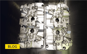
Blog
Leveraging Statistical Analysis Software in Advancing Material Efficiency with Pore Die Casting Read More

Read More
Blog
Closing the Control Gap Before Chiplets and Advanced Packaging Leave You BehindRead More

Read More
Blog
Battery Passport: Challenges & Opportunities in ManufacturingRead More

Read More
Press Release
camLine Launches the New Cornerstone 8.1 to Improve Users’ Data Analysis ExperienceRead More

Read More
camLine forum
camLine forum 2025Read More

Read More
Work Smarter
Integrating Recipe Management with Your MESRead More